More actions
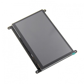
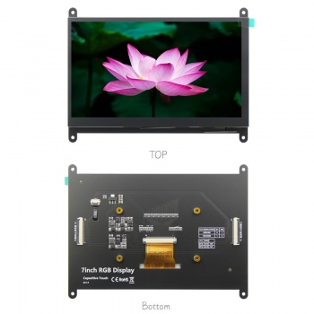
Product Picture
Product Description
- 7.0-inch color screen, support 24BIT RGB 16.7M color display, display rich colors
- Support 800x480 and 1024x600 resolution screen switching, the display effect is very clear
- Support 24 bit RGB parallel bus transmission
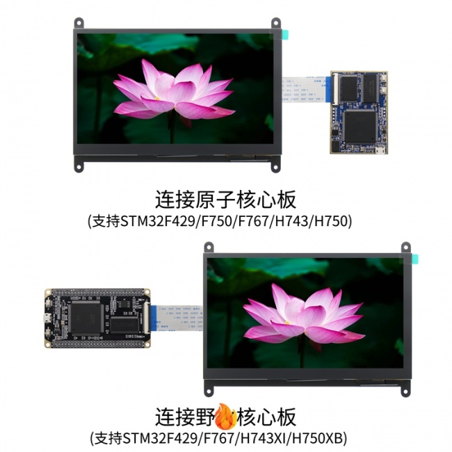
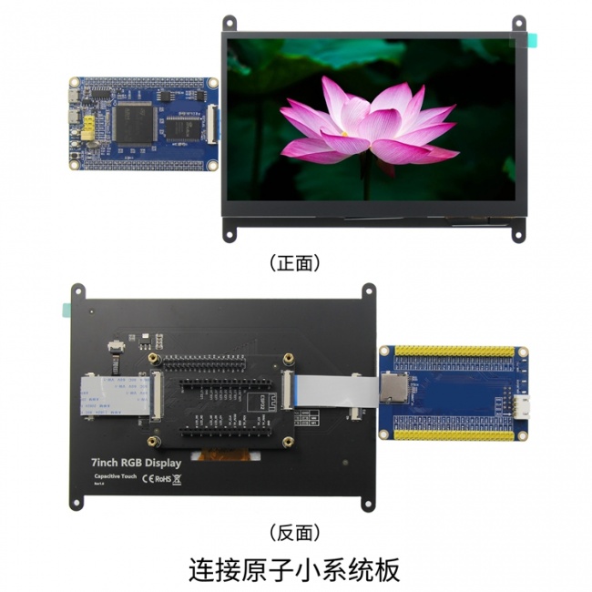
- Compatible with RGB interface connection of punctual atomic development board and wildfire development board
- Use capacitive touch screen to support 5 touch points
- Provides a rich sample program for STM32 platforms
- Military-grade process standards, long-term stable work
- Provide underlying driver technical support
Product Parameters
| Name | Parameter |
| Display Color | RGB888 16.7M (compatible with rgb5665k) color |
| SKU | 800x480:MRG7101(no touch), MRG7111(have touch)
1024x600:MRG7102(no touch),MRG7122(have touch) |
| Screen Size | 7.0(inch) |
| Type | TFT |
| Driver IC | None |
| Resolution | 800*480 or 1024x600 (Pixel) |
| Module Interface | 24Bit RGB parallel interface |
| Touch Screen Type | Capacitive touch screen |
| Touch IC | FT5426 |
| Active Area | 800x480: 153.84x85.63(mm)
1024x600: 154.21x85.92(mm) |
| Module PCB Size | 164.90x124.27(mm) |
| Operating Temperature | -20℃~60℃ |
| Storage Temperature | -30℃~70℃ |
| Input Voltage | 5V |
| IO Voltage | 3.3V |
| Power Consumption | 800x480: 67mA(The backlight is off), 467mA(The backlight is the brightest)
1024x600: 104mA(The backlight is off), 310mA(The backlight is the brightest) |
| Rough Weight(Net weight) | 236(g) |
Interface Definition
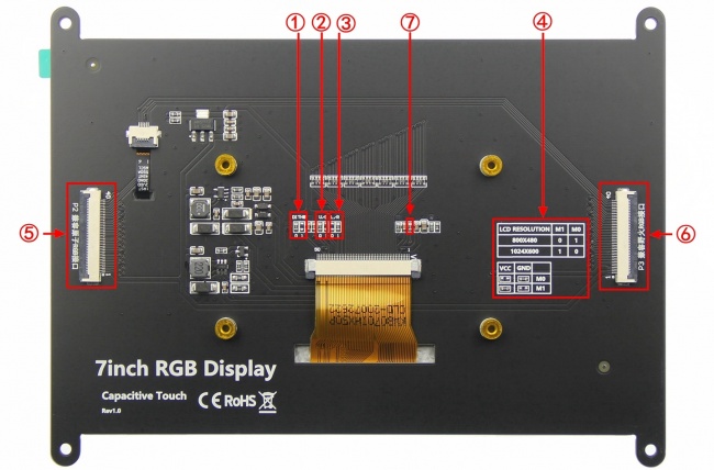
- ①--DITHB selection circuit
- ②--U/D selection circuit
- ③--L/R selection circuit
- ④--Screen resolution selection circuit
- ⑤--P2 interface (compatible with atomic RGB interface)
- ⑥--P3 interface (compatible with wildfire RGB interface)
- ⑦--B7 Data line pull resistance (required to define module ID, applicable to atomic program)
1. Screen internal Dithering display function settings
- Weld the 0 position resistance of DITHB and disconnect the 1 position resistance to enable the internal Dithering display function of the display panel;
- Weld the 1 position resistance of DITHB, disconnect the 0 position resistance, and turn off the internal Dithering display function of the screen;
- Default welding 0 position resistance, disconnect 1 position resistance
2. Screen display up and down flip settings
- Weld the resistance at position 0 of U / D, disconnect the resistance at position 1, and the screen will turn down;
- Weld the resistance at position 1 of U / D, disconnect the resistance at position 0, and the screen will turn upward;
- Default welding 0 position resistance, disconnect 1 position resistance
3. Screen display left and right flip settings
- weld the resistance at position 0 of L / R, disconnect the resistance at position 1, and the screen will turn to the left;
- Weld the resistance at position 1 of L / R, disconnect the resistance at position 0, and the screen will turn right;
- Default welding 1 position resistance, disconnect 0 position resistance
4. Screen resolution selection
- As shown in the screen resolution selection circuit, the module supports screen switching of 800x480 and 1024x600 resolutions.
- Weld M0 resistance to GND, M1 resistance to VCC, select 1024x600 resolution;
- Weld M0 resistance to VCC, M1 resistance to GND, and select 800x480 resolution;
5. Precautions for connecting to wildfire development board
- If connected to wildfire i When using the MX6ULL ARM Linux development board, it is necessary to remove the pull resistance
- on the B7 data line referred to by label 7 and the M0 and M1 resistance referred to by label 4, otherwise the development board will not run
6. P2 and P3 interface pins are described as follows:
- P2 interface (compatible with atomic RGB interface) pin description
| Number | Pin name | Description |
| 1 | VCC5 | Power input pin(connect to 5V) |
| 2 | VCC5 | Power input pin(connect to 5V) |
| 3~10 | R0~R7 | 8-bit RED data pin |
| 11 | GND | power ground pin |
| 12~19 | G0 ~ G7 | 8-bit GREEN data pin |
| 20 | GND | power ground pin |
| 21~28 | B0 ~ B7 | 8-bit GREEN data pin |
| 29 | GND | power ground pin |
| 30 | PCLK | Pixel clock control pin |
| 31 | HSYNC | Horizontal synchronous signal control pin |
| 32 | VSYNC | Vertical synchronous signal control pin |
| 33 | DE | Data enable signal control pin |
| 34 | BL | LCD backlight control pin |
| 35 | TP_CS | Capacitor touch screen reset pin (resistance touch screen chip selection pin) |
| 36 | TP_MOSI | Data pin of IIC bus of capacitance touch screen (write data pin of SPI bus of resistance touch screen) |
| 37 | TP_MISO | Resistance touch screen SPI bus read data pin (capacitance touch screen not used) |
| 38 | TP_CLK | IIC bus clock control pin of capacitive touch screen (SPI bus clock control pin of resistance touch screen) |
| 39 | TP_PEN | Touch screen interrupt control pin (low level when touch is generated) |
| 40 | RST | LCD reset control pin (effective at low level) |
- P3 interface (compatible with wildfire RGB interface) pin description
| Number | Pin name | Description |
| 1 | VCC5 | Power input pin(connect to 5V) |
| 2 | VCC5 | Power input pin(connect to 5V) |
| 3 | VCC3.3 | Power input pin(connect to 3.3V) |
| 4 | VCC3.3 | Power input pin(connect to 3.3V) |
| 5 | GND | power ground pin |
| 6~13 | R0 ~ R7 | 8-bit RED data pin |
| 14~21 | G0 ~ G7 | 8-bit GREEN data pin |
| 22~29 | B0 ~ B7 | 8-bit BLUE data pin |
| 30 | PCLK | Pixel clock control pin |
| 31 | HSYNC | Horizontal synchronous signal control pin |
| 32 | VSYNC | Vertical synchronous signal control pin |
| 33 | DE | Data enable signal control pin |
| 34 | DISP | LCD display enable pin (enable at high level, the module is not used) |
| 35 | BL | LCD backlight control pin |
| 36 | GND | power ground pin |
| 37 | TP_RST | Capacitor touch screen reset pin(enable at low level) |
| 38 | TP_PEN | Touch screen interrupt control pin (low level when touch is generated) |
| 39 | TP_SDA | Data pin of IIC bus of capacitance touch screen |
| 40 | TP_SCL | IIC bus clock control pin of capacitive touch screen |
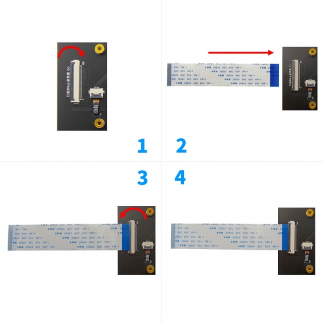
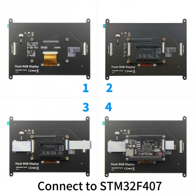
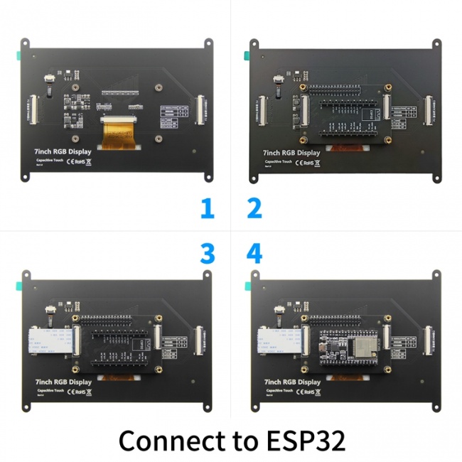
How to connect the development board
Program Download
Product Documentation
- 7.0inch RGB Display Module User Manual
- 7.0inch RGB IPS TFTLCD Specification
- 7.0inch RGB TN TFTLCD Specification
- 7.0inch RGB IPS TFTLCD RGB Timing
- 7.0inch RGB TN TFTLCD RGB Timing
- 7.0inch RGB Display Module Size Picture
- 7.0inch RGB Display Module Schematic
- 7.0inch RGB Display Module TFTLCD Schematic and PCB Package Library
- 7.0inch RGB IPS display driver IC data manual HX8282-A11
- 7.0inch RGB TN display driver IC data manual EK9716B
- Capacitance touch IC FT5426 Data sheet
- Capacitance touch IC FT5426 Programming Guide
Reference Materials
- STM32 keil software use illustration
- PCtoLCD2002 software use illustration
- Image2Lcd software use illustration
- Chinese and English display modulo settings

