More actions
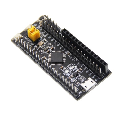
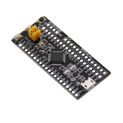
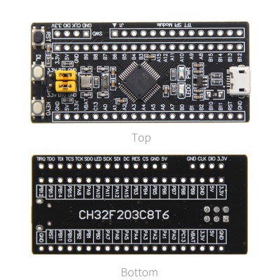
CH32F203C8T6 Development Board
Product Picture
Product Description
- CPU: CH32F203C8T6, the max main frequency: 144MHz, internal FLASH: 64KB, internal SRAM: 20KB
- Small and delicate appearance, convenient for various DIY projects
- Support USB, SWD and serial download, easy to debug
- Support SPI interface interface display module direct insertion
- Extended GPIO port for easy connection to various peripherals
- Rich development resources, easy to learn, easy to get started
Product Parameters
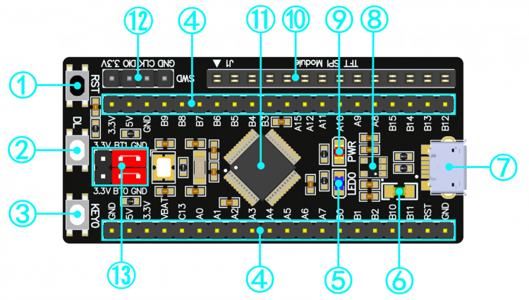
| Serial number | Name | Description |
| ① | RST reset button | Used to reset the development board by pressing the key |
| ② | DL download button | For USB Download and serial port download, press and hold the button, and then power on the smallest system board to enter the download mode |
| ③ | KEY0 test key | For standby wake-up or program key function design |
| ④ | Extended IO row pin | It is used to connect various peripherals to facilitate project development |
| ⑤ | Blue LED test light | Program running state for indication and DIY program lighting effect design |
| ⑥ | Self recovery fuse | It is used to ensure the safety of the circuit in case of short circuit or other faults |
| ⑦ | USB interface | Used for USB Download, USB communication, and power supply |
| ⑧ | 3.3V output voltage stabilizing IC | 5V input, 3.3V output |
| ⑨ | Red LED power indicator | Red LED light is used to indicate whether the development board is powered on normally |
| ⑩ | LCD in-line bus connector | Display module for in-line common-spi interface |
| ⑪ | STM32F203C8T6 | Main chip, maximum main frequency: 144mhz, internal flash:64kb, internal sram:20kb, supporting RTC, interrupt, PWM, DMA and other functions |
| ⑫ | SWD download and debugging interface | For SWD download, program debugging and simulation |
| ⑬ | BT0/BT1 start select port | Used to select the startup mode and download mode after the minimum system board is reset |
How to connect LCD screen
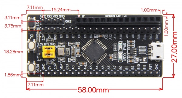
Product Size
Program Download
Product Documentation
- CH32F203C8T6 Minimum system board user manual
- CH32F203C8T6 Minimum system board size drawing
- CH32F203C8T6 minimum system board Schematic diagram
- CH32F203C8T6 Minimum system board IO resource allocation table
- CH32F203C8T6 Minimum system board schematic Library
- CH32F203C8T6 Minimum system board PCB package library
- CH32F203C8T6 Data Sheet
- CH32F2X Series application manual
Reference Materials
- CH32 development board SWD download instructions
- CH32 development board SWD download exception release read protection instructions
- CH32 development board serial port download instructions
- CH32 development board USB download instructions

