More actions
| (4 intermediate revisions by the same user not shown) | |||
| Line 84: | Line 84: | ||
==<font color="blue">Interface Definition</font> == | ==<font color="blue">Interface Definition</font> == | ||
[[File: | [[File:MRG4963-001.png|700px]] | ||
''' | '''Note:''' | ||
:A.The pins beginning with T are the relevant pins of the resistive touch screen; | |||
:B.The pins beginning with SD are SD card related pins; | |||
:C.Pins beginning with F are SPI flash related pins; | |||
:D.NC/ starts with relevant pins of capacitive touch screen; | |||
:E.The rest are LCD related pins; | |||
:F.SPI flash is not welded. If you need to use it, please weld it yourself; | |||
{| class="wikitable" border="1" style="width: 650px; background-color: white;" | {| class="wikitable" border="1" style="width: 650px; background-color: white;" | ||
|- | |||
| align="center" |Number | | align="center" |Number | ||
| align="center" |Pin | | align="center" |Pin Name | ||
| align="center" | | | align="center" |Pin Name | ||
|- | |- | ||
| align="center" |1 | | align="center" |1 | ||
| align="center" | | | align="center" |GND | ||
| | |power ground pin | ||
|- | |- | ||
| align="center" |2 | | align="center" |2 | ||
| align="center" | | | align="center" |3.3V | ||
| | |power positive pin(connected to 3.3V) | ||
|- | |- | ||
| align="center" |3 | | align="center" |3 | ||
| align="center" | | | align="center" |NC | ||
| | |Undefined, reserved | ||
|- | |- | ||
| align="center" |4 | | align="center" |4 | ||
| align="center" | | | align="center" |RS | ||
|LCD | |LCD register / data selection control pin (high level: register, low level: data) | ||
|- | |- | ||
| align="center" |5 | | align="center" |5 | ||
| align="center" | | | align="center" |WR | ||
|LCD | |LCD write control pin | ||
|- | |- | ||
| align="center" |6 | | align="center" |6 | ||
| align="center" | | | align="center" |RD | ||
|LCD read control pin | |||
|- | |- | ||
| align="center" |7 | | align="center" |7~14 | ||
| align="center" |DB8 ~ DB15 | |||
|LCD data bus high 8-bit pin | |||
| align="center" |DB8 | |||
|- | |- | ||
| align="center" |15 | | align="center" |15 | ||
| align="center" | | | align="center" |CS | ||
|LCD reset control pin( low level enable) | |||
|- | |- | ||
| align="center" |16 | | align="center" |16 | ||
| align="center" | | | align="center" |F_CS | ||
|SPI FLASH chip select control pin( low level enable) | |||
|- | |- | ||
| align="center" |17 | | align="center" |17 | ||
| align="center" | | | align="center" |REST | ||
|LCD reset control pin( low level reset) | |||
|- | |- | ||
| align="center" |18 | | align="center" |18 | ||
| align="center" | | | align="center" |NC | ||
|Undefined, reserved | |||
|- | |- | ||
| align="center" |19 | | align="center" |19 | ||
| align="center" | | | align="center" |LED_A | ||
|LCD backlight control pin(it needs to be used according to the selection) | |||
|- | |- | ||
| align="center" |20 | | align="center" |20 | ||
| align="center" | | | align="center" |NC/INT | ||
|There is no definition when connecting the resistance touch screen,Used as interrupt pin when connected to capacitive touch screen | |||
|- | |- | ||
| align="center" |21 | | align="center" |21~28 | ||
| align="center" | | | align="center" |DB0~DB7 | ||
|LCD data bus low 8-bit pin | |||
|- | |- | ||
| align="center" | | | align="center" |29 | ||
| align="center" | | | align="center" |T_CLK | ||
| | |Resistance touch screen SPI bus clock pin | ||
|- | |- | ||
| align="center" | | | align="center" |30 | ||
| align="center" | | | align="center" |T_CS | ||
| | |Resistive touch screen chip selection pin (low level enable) | ||
|- | |- | ||
| align="center" | | | align="center" |31 | ||
| align="center" | | | align="center" |T_DIN | ||
| | |Resistance touch screen SPI bus write data pin | ||
|- | |- | ||
| align="center" | | | align="center" |32 | ||
| align="center" | | | align="center" |NC/CRT | ||
|There is no definition when connecting the resistance touch screen,Used as reset pin when connected to capacitive touch screen (low level reset) | |||
|- | |- | ||
| align="center" | | | align="center" |33 | ||
| align="center" | | | align="center" |T_DO | ||
| | |Resistance touch screen SPI bus read data pin | ||
|- | |- | ||
| align="center" | | | align="center" |34 | ||
| align="center" | | | align="center" |T_IRQ | ||
|Resistance touch screen interrupt detection pin (active at low level) | |||
|- | |- | ||
| align="center" | | | align="center" |35 | ||
| align="center" | | | align="center" |SD_DO | ||
| | |SD card SDIO bus read data pin | ||
|- | |- | ||
| align="center" | | | align="center" |36 | ||
| align="center" | | | align="center" |SD_CLK | ||
| | |SD card SDIO bus clock pin | ||
|- | |- | ||
| align="center" | | | align="center" |37 | ||
| align="center" | | | align="center" |SD_DIN | ||
| | |SD card SDIO bus write data pin | ||
|- | |- | ||
| align="center" | | | align="center" |38 | ||
| align="center" | | | align="center" |SD_CS | ||
| | |SD card pin selection (low level enable) | ||
|- | |- | ||
| align="center" | | | align="center" |39 | ||
| align="center" | | | align="center" |NC/SDA | ||
| | |There is no definition when connecting the resistance touch screen,As IIC bus data pin when connected to capacitive touch screen | ||
|- | |- | ||
| align="center" | | | align="center" |40 | ||
| align="center" | | | align="center" |NC/SCL | ||
| | |There is no definition when connecting the resistance touch screen,Used as IIC bus clock pin when connected to capacitive touch screen | ||
|- | |- | ||
|} | |} | ||
==<font color="blue">Program Download</font> == | ==<font color="blue">Program Download</font> == | ||
* [http://www.lcdwiki.com/res/Program/Parallel_Port/4. | * [http://www.lcdwiki.com/res/Program/Parallel_Port/4.3inch/16BIT_SSD1963_MRB4963_V1.0/4.3inch_16BIT_Module_SSD1963_480x272_800x480_MRB4963_V1.0.zip '''4.3inch 16bit Parallel-Port Module package'''] | ||
==<font color="blue">Product Documentation</font> == | ==<font color="blue">Product Documentation</font> == | ||
* [http://www.lcdwiki.com/res/ | * [http://www.lcdwiki.com/res/MRB4963/User_Manual(Required_view).pdf '''4.3inch 16bit Parallel-Port Module User Manual'''] | ||
* [http://www.lcdwiki.com/res/ | * [http://www.lcdwiki.com/res/MRB4963/043JGI50_Specification.pdf '''4.3 inch IPS LCD specification'''] | ||
* [http://www.lcdwiki.com/ | * [http://www.lcdwiki.com/res/MRB4963/SPEC-4300J-V03.pdf '''4.3 inch TN LCD specification'''] | ||
* [http://www.lcdwiki.com/res/ | * [http://www.lcdwiki.com/res/MRB4963/4.3inch_SSD1963_display_Size.pdf '''4.3inch 16bit Parallel-Port Module size picture'''] | ||
* [http://www.lcdwiki.com/res/ | * [http://www.lcdwiki.com/res/MRB4963/4.3inch_SSD1963_display_Schematic.pdf '''4.3inch 16bit Parallel-Port Module Schematic'''] | ||
* [http://www.lcdwiki.com/res/ | * [http://www.lcdwiki.com/res/MRB4963/SSD1963_DS_V1.1.pdf '''SSD1963 data sheet'''] | ||
* [http://www.lcdwiki.com/res/MRB4963/XPT2046.pdf '''Resistance touch screen control IC data manual xpt2046'''] | |||
==<font color="blue">Reference Materials</font> == | ==<font color="blue">Reference Materials</font> == | ||
Latest revision as of 11:20, 15 July 2022
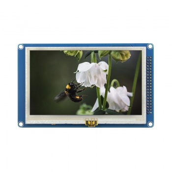
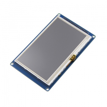
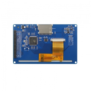
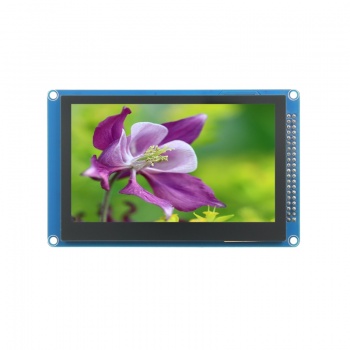
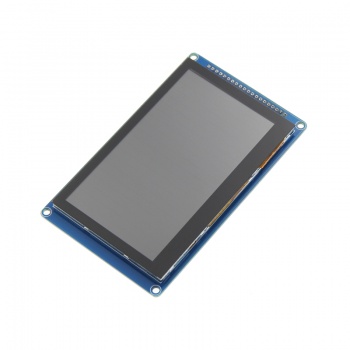
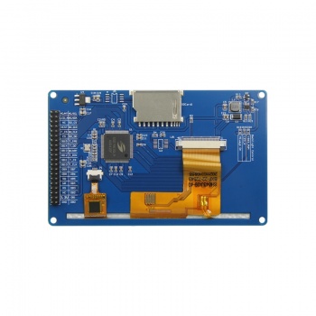
Product Picture
Product Description
- 4.3-inch high-definition color screen, supporting 16bit RGB 65K color display, with rich display colors
- Support IPS screen 800x480 resolution, and the display effect is very clear
- Support TN screen with 480x272 resolution and clear display effect
- Using 16-bit parallel bus transmission with fast transfer speed
- Compatible with capacitive touch screen and resistive touch screen
- Support SPI flash
- With SD card slot, support SD card expansion
- Support three backlight control modes (always on, GPIO control, PWM control)
- Provides a rich sample program for STM32 and C51 platforms
- Military-grade process standards, long-term stable work
- Provide underlying driver technical support
Product Parameters
| Name | Parameter |
| Display Color | 16BIT RGB 65K color |
| SKU | MRB4963 |
| Screen Size | 4.3(inch) |
| Screen Type | TFT |
| Driver IC | SSD1963 |
| Resolution | IPS: 800x480(Pixel)
TN: 480x272(Pixel) |
| Module Interface | 16Bit parallel interface |
| Active Area | 95.04.00x53.858(mm) |
| Touch Screen Type | Capacitive touch screen or Resistive touch screen |
| Touch IC | GT911 (capacitive touch), XPT2046 (resistive touch) |
| Module PCB Size | 120.00x74.00(mm) |
| Operating Temperature | -10℃~60℃ |
| Storage Temperature | -20℃~70℃ |
| Operating Voltage | 3.3V |
| IO Voltage | 3.3V |
| Power Consumption | TBD |
| Rough Weight(Package containing) | TBD |
Interface Definition
Note:
- A.The pins beginning with T are the relevant pins of the resistive touch screen;
- B.The pins beginning with SD are SD card related pins;
- C.Pins beginning with F are SPI flash related pins;
- D.NC/ starts with relevant pins of capacitive touch screen;
- E.The rest are LCD related pins;
- F.SPI flash is not welded. If you need to use it, please weld it yourself;
| Number | Pin Name | Pin Name |
| 1 | GND | power ground pin |
| 2 | 3.3V | power positive pin(connected to 3.3V) |
| 3 | NC | Undefined, reserved |
| 4 | RS | LCD register / data selection control pin (high level: register, low level: data) |
| 5 | WR | LCD write control pin |
| 6 | RD | LCD read control pin |
| 7~14 | DB8 ~ DB15 | LCD data bus high 8-bit pin |
| 15 | CS | LCD reset control pin( low level enable) |
| 16 | F_CS | SPI FLASH chip select control pin( low level enable) |
| 17 | REST | LCD reset control pin( low level reset) |
| 18 | NC | Undefined, reserved |
| 19 | LED_A | LCD backlight control pin(it needs to be used according to the selection) |
| 20 | NC/INT | There is no definition when connecting the resistance touch screen,Used as interrupt pin when connected to capacitive touch screen |
| 21~28 | DB0~DB7 | LCD data bus low 8-bit pin |
| 29 | T_CLK | Resistance touch screen SPI bus clock pin |
| 30 | T_CS | Resistive touch screen chip selection pin (low level enable) |
| 31 | T_DIN | Resistance touch screen SPI bus write data pin |
| 32 | NC/CRT | There is no definition when connecting the resistance touch screen,Used as reset pin when connected to capacitive touch screen (low level reset) |
| 33 | T_DO | Resistance touch screen SPI bus read data pin |
| 34 | T_IRQ | Resistance touch screen interrupt detection pin (active at low level) |
| 35 | SD_DO | SD card SDIO bus read data pin |
| 36 | SD_CLK | SD card SDIO bus clock pin |
| 37 | SD_DIN | SD card SDIO bus write data pin |
| 38 | SD_CS | SD card pin selection (low level enable) |
| 39 | NC/SDA | There is no definition when connecting the resistance touch screen,As IIC bus data pin when connected to capacitive touch screen |
| 40 | NC/SCL | There is no definition when connecting the resistance touch screen,Used as IIC bus clock pin when connected to capacitive touch screen |
Program Download
Product Documentation
- 4.3inch 16bit Parallel-Port Module User Manual
- 4.3 inch IPS LCD specification
- 4.3 inch TN LCD specification
- 4.3inch 16bit Parallel-Port Module size picture
- 4.3inch 16bit Parallel-Port Module Schematic
- SSD1963 data sheet
- Resistance touch screen control IC data manual xpt2046
Reference Materials
- C51 Keil and stc-isp software use illustration
- STM32 keil software use illustration
- PCtoLCD2002 software use illustration
- Image2Lcd software use illustration
- Chinese and English display modulo settings

