More actions
| Line 69: | Line 69: | ||
{| class="wikitable" border="1" style="width: 600px; background-color: white;" | {| class="wikitable" border="1" style="width: 600px; background-color: white;" | ||
|- | |- | ||
| align="center" | | | align="center" |Number | ||
| align="center" | | | align="center" |Pin name | ||
| align="center" | | | align="center" |Description | ||
|- | |- | ||
| align="center" |1 | | align="center" |1 | ||
| align="center" |CS | | align="center" |CS | ||
| | |LCD reset control pin( low level enable) | ||
|- | |- | ||
| align="center" |2 | | align="center" |2 | ||
| align="center" |RS | | align="center" |RS | ||
| | |LCD register / data selection control pin(high level: register, low level: data) | ||
|- | |- | ||
| align="center" |3 | | align="center" |3 | ||
| align="center" |WR | | align="center" |WR | ||
| | |LCD write control pin | ||
|- | |- | ||
| align="center" |4 | | align="center" |4 | ||
| align="center" |RD | | align="center" |RD | ||
| | |LCD read control pin | ||
|- | |- | ||
| align="center" |5 | | align="center" |5 | ||
| align="center" |RST | | align="center" |RST | ||
| | |LCD reset control pin( low level reset) | ||
|- | |- | ||
| align="center" |6~21 | | align="center" |6~21 | ||
| align="center" |D0~D15 | | align="center" |D0~D15 | ||
| | |LCD 16 bit data bus pin (use d0 ~ D7 in 8-bit mode) | ||
|- | |- | ||
| align="center" |22 | | align="center" |22 | ||
| align="center" |GND | | align="center" |GND | ||
| | |Module power ground pin | ||
|- | |- | ||
| align="center" |23 | | align="center" |23 | ||
| align="center" |TE | | align="center" |TE | ||
| | |LCD tearing effect signal pin (read only) | ||
|- | |- | ||
| align="center" |24 | | align="center" |24 | ||
| align="center" |NC | | align="center" |NC | ||
| | |No definition, reserved | ||
|- | |- | ||
| align="center" |25 | | align="center" |25 | ||
| align="center" |NC | | align="center" |NC | ||
| | |No definition, reserved | ||
|- | |- | ||
| align="center" |26 | | align="center" |26 | ||
| align="center" |GND | | align="center" |GND | ||
| | |Module power ground pin | ||
|- | |- | ||
| align="center" |27 | | align="center" |27 | ||
| align="center" |GND | | align="center" |GND | ||
| | |Module power ground pin | ||
|- | |- | ||
| align="center" |28 | | align="center" |28 | ||
| align="center" |5V | | align="center" |5V | ||
| | |Module power supply positive pin (connected to 5V) | ||
|- | |- | ||
| align="center" |29 | | align="center" |29 | ||
| align="center" |TMI | | align="center" |TMI | ||
| | |Resistance touch screen SPI bus read data pin (capacitor touch screen not used) | ||
|- | |- | ||
| align="center" |30 | | align="center" |30 | ||
| align="center" |TMO | | align="center" |TMO | ||
| | |IIC bus data pin of capacitive touch screen (SPI bus write data pin of resistance touch screen) | ||
|- | |- | ||
| align="center" |31 | | align="center" |31 | ||
| align="center" |PEN | | align="center" |PEN | ||
| | |Touch screen interrupt detection pin(Low level when a touch occurs) | ||
|- | |- | ||
| align="center" |32 | | align="center" |32 | ||
| align="center" |NC | | align="center" |NC | ||
| | |No definition, reserved | ||
|- | |- | ||
| align="center" |33 | | align="center" |33 | ||
| align="center" |TCS | | align="center" |TCS | ||
| | |Capacitor touch screen reset pin (resistance touch screen chip selection pin) | ||
|- | |- | ||
| align="center" |34 | | align="center" |34 | ||
| align="center" |TCK | | align="center" |TCK | ||
| | |IIC bus clock pin of capacitive touch screen (SPI bus clock pin of resistance touch screen) | ||
|- | |- | ||
|} | |} | ||
*''' | *'''STM32 development board flexible cable input interface pin description''' | ||
{| class="wikitable" border="1" style="width: 600px; background-color: white;" | {| class="wikitable" border="1" style="width: 600px; background-color: white;" | ||
|- | |- | ||
| align="center" | | | align="center" |Number | ||
| align="center" | | | align="center" |Pin name | ||
| align="center" | | | align="center" |Description | ||
|- | |- | ||
| align="center" |1 | | align="center" |1 | ||
| align="center" |TCK | | align="center" |TCK | ||
| | |IIC bus clock pin of capacitive touch screen (SPI bus clock pin of resistance touch screen) | ||
|- | |- | ||
| align="center" |2 | | align="center" |2 | ||
| align="center" |TCS | | align="center" |TCS | ||
| | |Capacitor touch screen reset pin (resistance touch screen chip selection pin) | ||
|- | |- | ||
| align="center" |3 | | align="center" |3 | ||
| align="center" |PEN | | align="center" |PEN | ||
| | |Touch screen interrupt detection pin(Low level when a touch occurs) | ||
|- | |- | ||
| align="center" |4 | | align="center" |4 | ||
| align="center" |TMO | | align="center" |TMO | ||
| | |IIC bus data pin of capacitive touch screen (SPI bus write data pin of resistance touch screen) | ||
|- | |- | ||
| align="center" |5 | | align="center" |5 | ||
| align="center" |TMI | | align="center" |TMI | ||
| | |Resistance touch screen SPI bus read data pin (capacitor touch screen not used) | ||
|- | |- | ||
| align="center" |6 | | align="center" |6 | ||
| align="center" |5V | | align="center" |5V | ||
| | |Module power supply positive pin (connected to 5V) | ||
|- | |- | ||
| align="center" |7 | | align="center" |7 | ||
| align="center" |GND | | align="center" |GND | ||
| | |Module power ground pin | ||
|- | |- | ||
| align="center" |8 | | align="center" |8 | ||
| align="center" |GND | | align="center" |GND | ||
| | |Module power ground pin | ||
|- | |- | ||
| align="center" |9 | | align="center" |9 | ||
| align="center" |NC | | align="center" |NC | ||
| | |No definition, reserved | ||
|- | |- | ||
| align="center" |10 | | align="center" |10 | ||
| align="center" |NC | | align="center" |NC | ||
| | |No definition, reserved | ||
|- | |- | ||
| align="center" |11 | | align="center" |11 | ||
| align="center" |TE | | align="center" |TE | ||
| | |LCD tearing effect signal pin (read only) | ||
|- | |- | ||
| align="center" |12~27 | | align="center" |12~27 | ||
| align="center" |D15~D0 | | align="center" |D15~D0 | ||
| | |LCD 16 bit data bus pin (use d0 ~ D7 in 8-bit mode) | ||
|- | |- | ||
| align="center" |28 | | align="center" |28 | ||
| align="center" |RST | | align="center" |RST | ||
| | |LCD reset control pin( low level reset) | ||
|- | |- | ||
| align="center" |29 | | align="center" |29 | ||
| align="center" |RD | | align="center" |RD | ||
| | |LCD read control pin | ||
|- | |- | ||
| align="center" |30 | | align="center" |30 | ||
| align="center" |WR | | align="center" |WR | ||
| | |LCD write control pin | ||
|- | |- | ||
| align="center" |31 | | align="center" |31 | ||
| align="center" |RS | | align="center" |RS | ||
| | |LCD register / data selection control pin(high level: register, low level: data) | ||
|- | |- | ||
| align="center" |32 | | align="center" |32 | ||
| align="center" |CS | | align="center" |CS | ||
| | |LCD reset control pin( low level enable) | ||
|- | |- | ||
|} | |} | ||
*''' | *'''ESP32 development board''' '''in line interface pin description''' | ||
{| class="wikitable" border="1" style="width: 600px; background-color: white;" | {| class="wikitable" border="1" style="width: 600px; background-color: white;" | ||
|- | |- | ||
| align="center" | | | align="center" |Number | ||
| align="center" | | | align="center" |Pin name | ||
| align="center" | | | align="center" |Description | ||
|- | |- | ||
| align="center" |1 | | align="center" |1 | ||
| align="center" |5V | | align="center" |5V | ||
| | |power pin (connected to 5V) | ||
|- | |- | ||
| align="center" |2 | | align="center" |2 | ||
| align="center" |LCD_RS | | align="center" |LCD_RS | ||
| | |LCD register / data selection control pin(high level: register, low level: data) | ||
|- | |- | ||
| align="center" |3 | | align="center" |3 | ||
| align="center" |LCD_RD | | align="center" |LCD_RD | ||
| | |LCD read control pin | ||
|- | |- | ||
| align="center" |4 | | align="center" |4 | ||
| align="center" |LCD_D1 | | align="center" |LCD_D1 | ||
| | |Pin 2 of 8-bit parallel data bus | ||
|- | |- | ||
| align="center" |5 | | align="center" |5 | ||
| align="center" |GND | | align="center" |GND | ||
| | |Power ground pin | ||
|- | |- | ||
| align="center" |6 | | align="center" |6 | ||
| align="center" |LCD_WR | | align="center" |LCD_WR | ||
| | |LCD write control pin | ||
|- | |- | ||
| align="center" |7 | | align="center" |7 | ||
| align="center" |LCD_D0 | | align="center" |LCD_D0 | ||
| | |Pin 1 of 8-bit parallel data bus | ||
|- | |- | ||
| align="center" |8 | | align="center" |8 | ||
| align="center" |LCD_D5 | | align="center" |LCD_D5 | ||
| | |Pin 6 of 8-bit parallel data bus | ||
|- | |- | ||
| align="center" |9 | | align="center" |9 | ||
| align="center" |LCD_D7 | | align="center" |LCD_D7 | ||
| | |Pin 8 of 8-bit parallel data bus | ||
|- | |- | ||
| align="center" |10 | | align="center" |10 | ||
| align="center" |LCD_D4 | | align="center" |LCD_D4 | ||
| | |Pin 5 of 8-bit parallel data bus | ||
|- | |- | ||
| align="center" |11 | | align="center" |11 | ||
| align="center" |LCD_D6 | | align="center" |LCD_D6 | ||
| | |Pin 7 of 8-bit parallel data bus | ||
|- | |- | ||
| align="center" |12 | | align="center" |12 | ||
| align="center" |LCD_D2 | | align="center" |LCD_D2 | ||
| | |Pin 3 of 8-bit parallel data bus | ||
|- | |- | ||
| align="center" |13 | | align="center" |13 | ||
| align="center" |TP_CLK | | align="center" |TP_CLK | ||
| | |IIC bus clock control pin of capacitive touch screen(SPI bus clock control pin of resistance touch screen) | ||
|- | |- | ||
| align="center" |14 | | align="center" |14 | ||
| align="center" |LCD_D3 | | align="center" |LCD_D3 | ||
| | |Pin 4 of 8-bit parallel data bus | ||
|- | |- | ||
| align="center" |15 | | align="center" |15 | ||
| align="center" |TP_MISO | | align="center" |TP_MISO | ||
| | |SPI bus read data pin of resistance touch screen(capacitive touch screen not used) | ||
|- | |- | ||
| align="center" |16 | | align="center" |16 | ||
| align="center" |LCD_CS | | align="center" |LCD_CS | ||
| | |LCD chip select control pin | ||
|- | |- | ||
| align="center" |17 | | align="center" |17 | ||
| align="center" |GND | | align="center" |GND | ||
| | |Power ground pin | ||
|- | |- | ||
| align="center" |18 | | align="center" |18 | ||
| align="center" |LCD_RST | | align="center" |LCD_RST | ||
| | |LCD reset control pin | ||
|- | |- | ||
| align="center" |19 | | align="center" |19 | ||
| align="center" |TP_PEN | | align="center" |TP_PEN | ||
| | |Touch screen interrupt control pin | ||
|- | |- | ||
| align="center" |20 | | align="center" |20 | ||
| align="center" |TE | | align="center" |TE | ||
| | |Tearing Effect Signal pin(read-only) | ||
|- | |- | ||
| align="center" |21 | | align="center" |21 | ||
| align="center" |TP_CS | | align="center" |TP_CS | ||
| | |Capacitive touch screen reset pin(resistance touch screen chip selection pin) | ||
|- | |- | ||
| align="center" |22 | | align="center" |22 | ||
| align="center" |TP_MOSI | | align="center" |TP_MOSI | ||
| | |IIC bus data pin of capacitive touch screen(resistance touch screen SPI bus write data pin) | ||
|- | |- | ||
| align="center" |23 | | align="center" |23 | ||
| align="center" |GND | | align="center" |GND | ||
| | |Power ground pin | ||
|- | |- | ||
|} | |} | ||
Revision as of 10:51, 8 January 2021
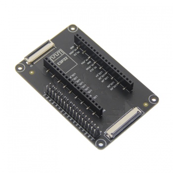
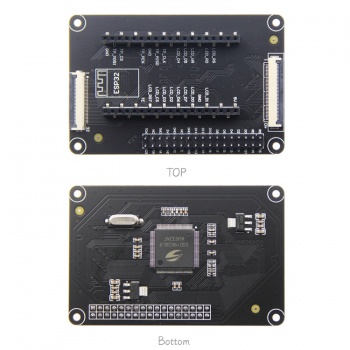
Product Picture
Product Description
- The ssd1963 control IC is On board
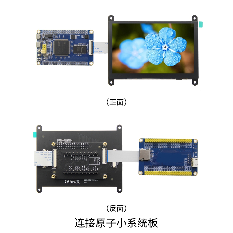
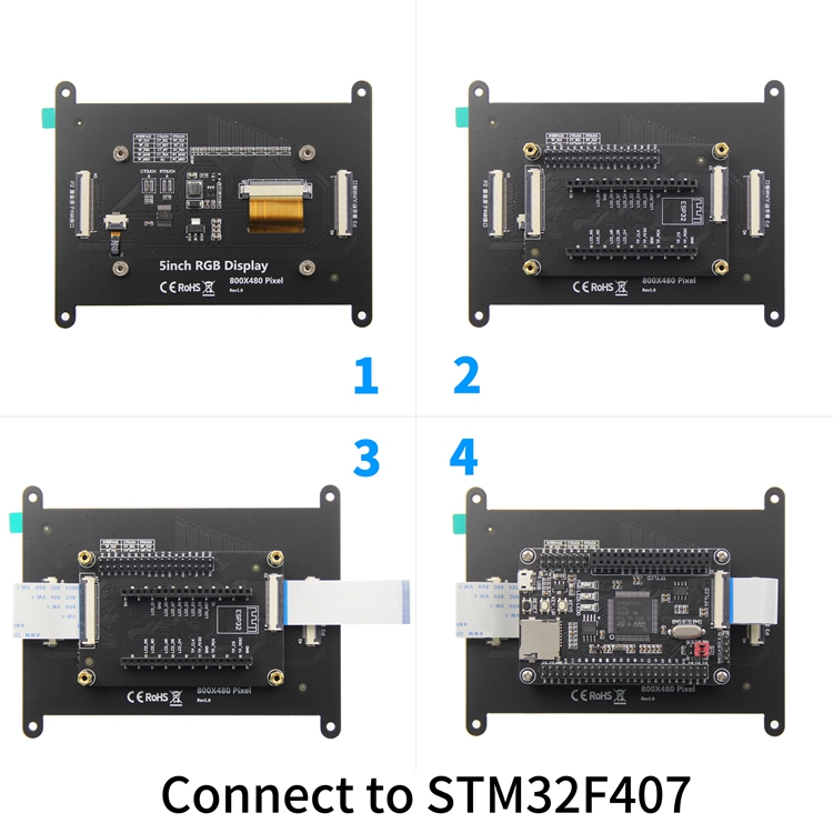
- Support the direct connection of flexible cable and needle of STM32 development board
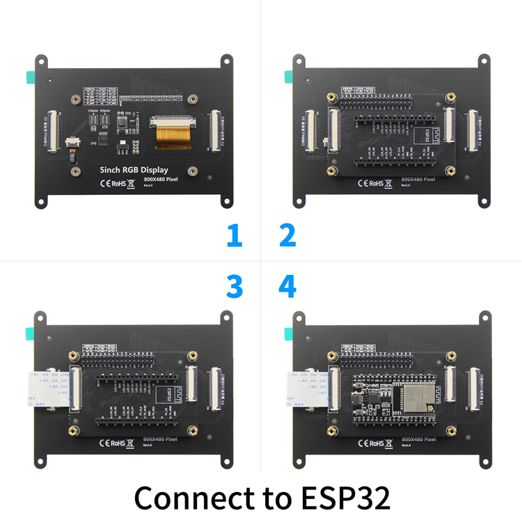
- Support direct insertion of esp32 development board
- Support direct connection of RGB display module flexible cable
- Support 8-bit and 16 bit parallel bus transmission, transmission speed block
- Provide rich STM32 platform and esp32 platform sample program
- Military grade process standard, long-term stable work
- Provide technical support for underlying driver
Product Parameters
| Name | Parameter |
| SKU | SSD1963 |
| Driver IC | SSD1963 |
| STM32 development board input interface | 16 bit parallel port |
| Input interface of esp32 development board | 8 bit parallel port |
| Output interface | 24 bit RGB parallel port |
| Module PCB Size | 50.00x77.00(mm) |
| Input Voltage | 5V |
| IO Voltage | 3.3V and 1.8V |
| Power Consumption | 36mA |
| Rough Weight(Net weight) | 22 (g) |
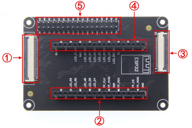
Interface Definition
- ①--40pin flexible cable output interface
- ②④--In line interface of esp32 development board
- ③--STM32 development board 32pin flexible cable input interface
- ⑤--STM32 development board 34pin pin input interface
- STM32 development board row pin input interface pin description
| Number | Pin name | Description |
| 1 | CS | LCD reset control pin( low level enable) |
| 2 | RS | LCD register / data selection control pin(high level: register, low level: data) |
| 3 | WR | LCD write control pin |
| 4 | RD | LCD read control pin |
| 5 | RST | LCD reset control pin( low level reset) |
| 6~21 | D0~D15 | LCD 16 bit data bus pin (use d0 ~ D7 in 8-bit mode) |
| 22 | GND | Module power ground pin |
| 23 | TE | LCD tearing effect signal pin (read only) |
| 24 | NC | No definition, reserved |
| 25 | NC | No definition, reserved |
| 26 | GND | Module power ground pin |
| 27 | GND | Module power ground pin |
| 28 | 5V | Module power supply positive pin (connected to 5V) |
| 29 | TMI | Resistance touch screen SPI bus read data pin (capacitor touch screen not used) |
| 30 | TMO | IIC bus data pin of capacitive touch screen (SPI bus write data pin of resistance touch screen) |
| 31 | PEN | Touch screen interrupt detection pin(Low level when a touch occurs) |
| 32 | NC | No definition, reserved |
| 33 | TCS | Capacitor touch screen reset pin (resistance touch screen chip selection pin) |
| 34 | TCK | IIC bus clock pin of capacitive touch screen (SPI bus clock pin of resistance touch screen) |
- STM32 development board flexible cable input interface pin description
| Number | Pin name | Description |
| 1 | TCK | IIC bus clock pin of capacitive touch screen (SPI bus clock pin of resistance touch screen) |
| 2 | TCS | Capacitor touch screen reset pin (resistance touch screen chip selection pin) |
| 3 | PEN | Touch screen interrupt detection pin(Low level when a touch occurs) |
| 4 | TMO | IIC bus data pin of capacitive touch screen (SPI bus write data pin of resistance touch screen) |
| 5 | TMI | Resistance touch screen SPI bus read data pin (capacitor touch screen not used) |
| 6 | 5V | Module power supply positive pin (connected to 5V) |
| 7 | GND | Module power ground pin |
| 8 | GND | Module power ground pin |
| 9 | NC | No definition, reserved |
| 10 | NC | No definition, reserved |
| 11 | TE | LCD tearing effect signal pin (read only) |
| 12~27 | D15~D0 | LCD 16 bit data bus pin (use d0 ~ D7 in 8-bit mode) |
| 28 | RST | LCD reset control pin( low level reset) |
| 29 | RD | LCD read control pin |
| 30 | WR | LCD write control pin |
| 31 | RS | LCD register / data selection control pin(high level: register, low level: data) |
| 32 | CS | LCD reset control pin( low level enable) |
- ESP32 development board in line interface pin description
| Number | Pin name | Description |
| 1 | 5V | power pin (connected to 5V) |
| 2 | LCD_RS | LCD register / data selection control pin(high level: register, low level: data) |
| 3 | LCD_RD | LCD read control pin |
| 4 | LCD_D1 | Pin 2 of 8-bit parallel data bus |
| 5 | GND | Power ground pin |
| 6 | LCD_WR | LCD write control pin |
| 7 | LCD_D0 | Pin 1 of 8-bit parallel data bus |
| 8 | LCD_D5 | Pin 6 of 8-bit parallel data bus |
| 9 | LCD_D7 | Pin 8 of 8-bit parallel data bus |
| 10 | LCD_D4 | Pin 5 of 8-bit parallel data bus |
| 11 | LCD_D6 | Pin 7 of 8-bit parallel data bus |
| 12 | LCD_D2 | Pin 3 of 8-bit parallel data bus |
| 13 | TP_CLK | IIC bus clock control pin of capacitive touch screen(SPI bus clock control pin of resistance touch screen) |
| 14 | LCD_D3 | Pin 4 of 8-bit parallel data bus |
| 15 | TP_MISO | SPI bus read data pin of resistance touch screen(capacitive touch screen not used) |
| 16 | LCD_CS | LCD chip select control pin |
| 17 | GND | Power ground pin |
| 18 | LCD_RST | LCD reset control pin |
| 19 | TP_PEN | Touch screen interrupt control pin |
| 20 | TE | Tearing Effect Signal pin(read-only) |
| 21 | TP_CS | Capacitive touch screen reset pin(resistance touch screen chip selection pin) |
| 22 | TP_MOSI | IIC bus data pin of capacitive touch screen(resistance touch screen SPI bus write data pin) |
| 23 | GND | Power ground pin |
- 软排线输出接口引脚说明
| 序号 | 引脚名称 | 说明 |
| 1 | VCC5 | 电源输入引脚(接5V) |
| 2 | VCC5 | 电源输入引脚(接5V) |
| 3~10 | R0~R7 | 8位RED数据引脚 |
| 11 | GND | 电源地 |
| 12~19 | G0 ~ G7 | 8位GREEN数据引脚 |
| 20 | GND | 电源地 |
| 21~28 | B0 ~ B7 | 8位BLUE数据引脚 |
| 29 | GND | 电源地 |
| 30 | PCLK | 像素时钟控制引脚 |
| 31 | HSYNC | 水平同步信号控制引脚 |
| 32 | VSYNC | 垂直同步信号控制引脚 |
| 33 | DE | 数据使能信号控制引脚 |
| 34 | LCD_BL | 液晶屏背光控制引脚 |
| 35 | TP_CS | 电容触摸屏复位引脚(电阻触摸屏片选引脚) |
| 36 | TP_MOSI | 电容触摸屏IIC总线数据引脚(电阻触摸屏SPI总线写数据引脚) |
| 37 | TP_MISO | 电阻触摸屏SPI总线读数据引脚(电容触摸屏没使用) |
| 38 | TP_CLK | 电容触摸屏IIC总线时钟控制引脚(电阻触摸屏SPI总线时钟控制引脚) |
| 39 | TP_PEN | 触摸屏中断控制引脚(产生触摸时,为低电平) |
| 40 | LCD_RST | 液晶屏复位控制引脚(低电平有效) |

